


범주
추천 제품

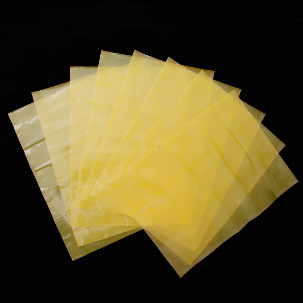
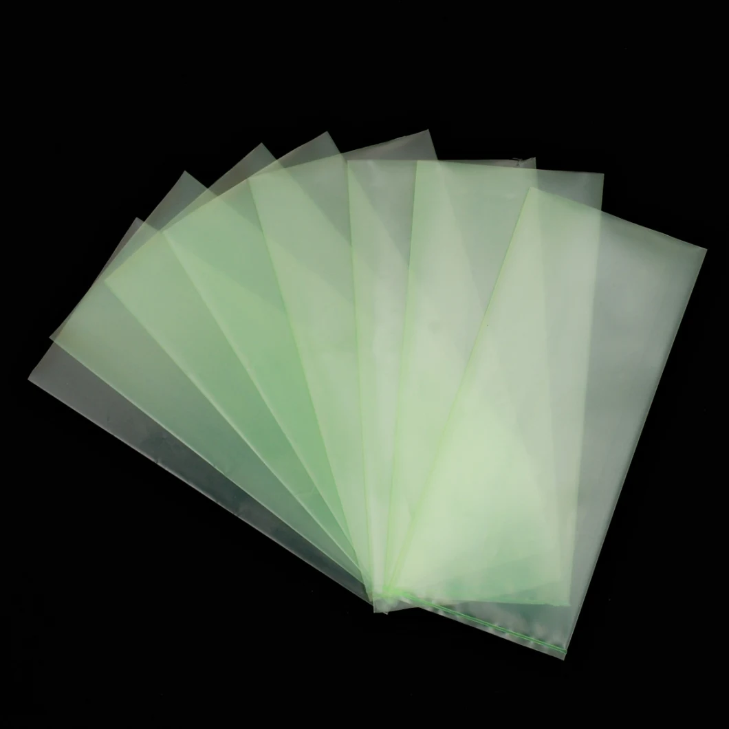
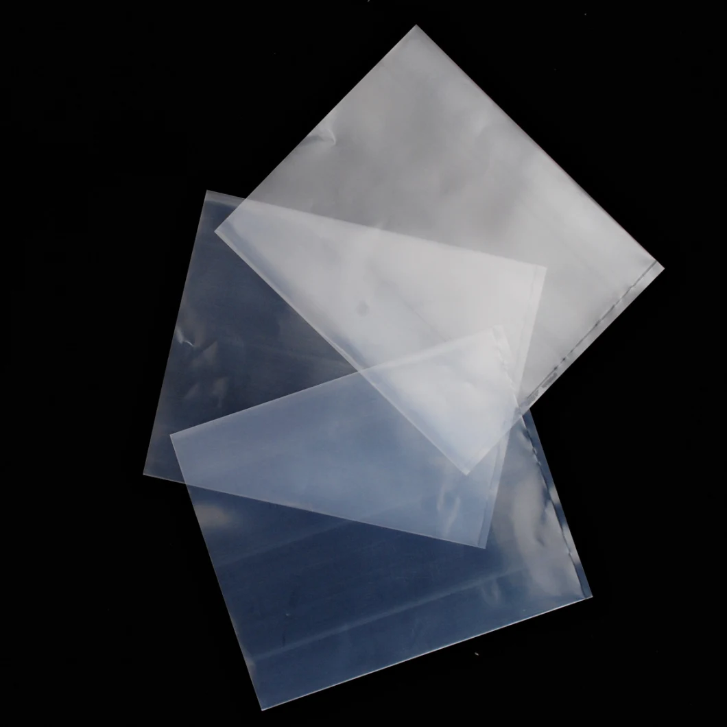
전자 반도체 및 폴리실리콘 포장재용 플라스틱 ESD PE 백
설명: 클린룸 백은 더 큰 보호를 위해 열 밀봉이 가능한 비부식성 폴리에틸렌 백입니다. 가방의 특징은 실리콘 프리, 아미드 프리, 환경 친화적이며
기본정보
| 모델 번호. | 해당 없음 |
| 처리 유형 | 드라이 라미네이션 |
| 크기 | 맞춤형 |
| 누르다 | 맞춤형 |
| 색상 | 맞춤형 |
| 두께 | 맞춤형 |
| 운송 패키지 | 팔레트 |
| 사양 | SGS RoHS 보고서 |
| 등록 상표 | 그을린 |
| 기원 | 중국 쑤저우 |
| HS 코드 | 3920999090 |
| 생산 능력 | 800톤/월 |
상품 설명
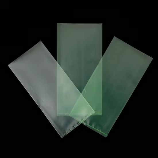
설명:클린룸 백은 더 큰 보호를 위해 열 밀봉이 가능한 비부식성 폴리에틸렌 백입니다.
가방의 특징은 무실리콘, 무아미드, 환경친화적, 무용제입니다.
당사의 재밀봉 가능한 가방은 내구성이 매우 뛰어나고 정전기에 민감한 전자 제품을 보관하는 데 이상적입니다. 이 투명 백을 사용하면 내용물을 쉽게 식별할 수 있고 먼지와 습기로부터 보호할 수 있습니다. 귀하의 로고로 맞춤 인쇄가 가능합니다.
| 상품명 | 가방에 |
| 원료 | 스포츠 |
| 색상 | 핑크, 클라, 블루... |
| 크기 | 맞춤형 |
| 포켓 스타일 | 지퍼락, 개방형 |
| 두께 | 20-200 마이크로미터 |
| 사용 | 모든 종류의 품목을 포장하는 데 사용할 수 있습니다. |
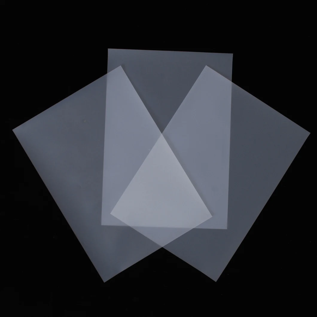
제품 보기:
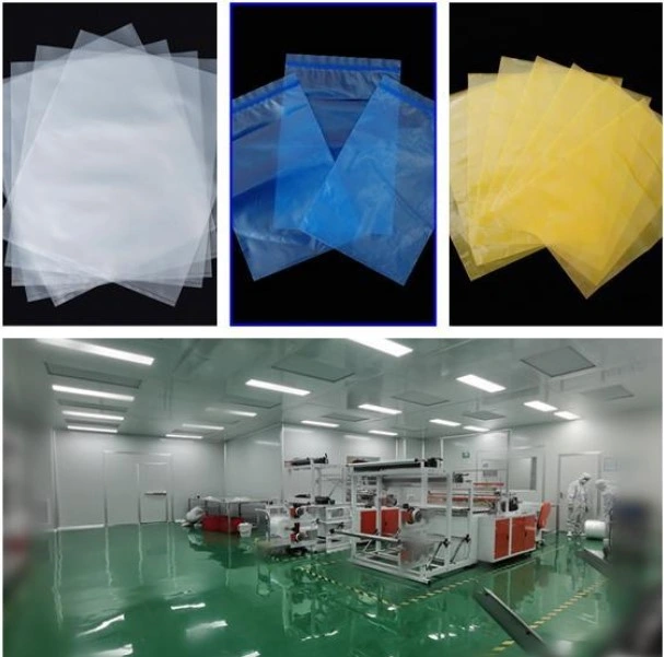
공장 쇼:
요청을 받는 방법:
개별 포장으로 배송해 드립니다. 정확한 가격을 알려드리기 위해 다음 사항을 알려주시기 바랍니다. 1. 수량, 2. 소재 및 두께 및 색상 3. 크기(L*W*H) 4. 인쇄(인쇄가 필요한 경우): 색상 수와 원하는 색상 단면 또는 양면에 인쇄하고 싶습니까? 5. 네, 비슷한 참고 이미지가 있으면 더 좋습니다. 6. 무역 유형: 우리는 일반적으로 FOB 조건을 사용하지만 CIF, DDU 등도 사용할 수 있습니다.
샘플을 얻는 방법:
After confirmation of inquiry, If need the sample.1. If you only need the similar sample, it will be free of charge.You only need to pay the freight. or provide your Fedex no.2..If you need the customized sample, there will be about usd50-500 sample fee, which will be calculated according to your product requirements; (orders will be returned if the quantity is large,Pls. contact the customer service).*Special note: if you only need a few thousand bags but need to make a sample, maybe the sample fee is closed to the cost of producing several thousand bags